Careers at ETL
Let’s work together to create success
Our company is on the lookout for highly motivated individuals who are dedicated to their craft and are eager to join our teams to help us expand and diversify our business. We are actively seeking passionate individuals to work with us, and our teams are dedicated to different aspects of the business.
We offer opportunities for people at all stages of their careers, from experienced professionals to fresh graduates, with a variety of roles available to fit the right candidate. If you are enthusiastic about your work and willing to help us grow and become more diverse, we would love to have you as part of our team.
We are currently interviewing for the following positions.
| Manufacturing Technician | Hook, UK |
| Junior RF Engineer | Rickmansworth, UK |
| Senior Mechanical Design Engineer | Rickmansworth, UK |
| Test Engineer | Hereford, UK |
| Systems Engineer Draughtsperson | Hereford, UK |
| Principal RF Engineer (Q&V Band) | Hereford or Rickmansworth, UK |
| PCB Design Engineer | Hereford or Rickmansworth, UK |
| Principal Product Systems Engineer | Hereford or Rickmansworth, UK |
| Senior Product Systems Engineer | Hereford or Rickmansworth, UK |
| Cleaning Operative (Part Time) | Hereford, UK |
Unlock your potential and seize the opportunity to apply for your dream job today!
Click here to apply and take the first step towards a promising career.
Early Careers
Are you ready to kickstart your career in Engineering and Manufacturing? Look no further than ETL Systems’ Early Careers Programme! This fantastic initiative is designed to help budding engineers and professionals gain invaluable experience in the industry.
Whether you’re still in school, fresh out of university, or somewhere in between, there’s something here for you.
| University Internship Opportunities | Hereford, UK |
| Manufacturing Summer Internship | Hereford, UK |
| Work Experience – Engineering / Manufacturing / Supply, Logistics & Operations / Finance, IT & Human Resources / Sales & Marketing | Hereford, UK |
Employee Benefits
At ETL, we prioritise taking care of our employees. We take pride in our exceptional benefits package that provides a flexible and healthy work environment.
Speculative Applications Welcome
As our company expands, we are constantly searching for skilled and passionate professionals who want to join our amazing team! If you’re interested in registering your CV with our Talent team, kindly submit your speculative CV directly through the link here: Speculative CV upload
Our People Make Us World Leaders
in RF & Satellite Communications

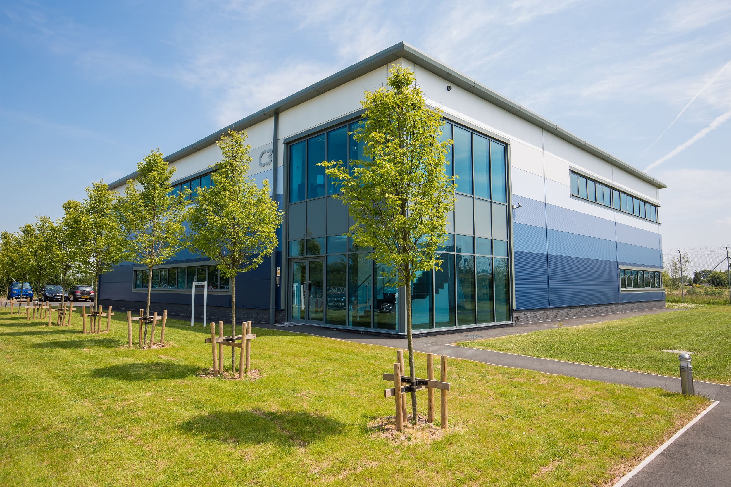
ETL Systems has been at the forefront of RF design and manufacturing for over 35 years. It designs and builds essential elements of critical satellite communications infrastructure. Its culture of innovation and its solutioneering approach have established it as a market leader in the field, with revenue growing 30x since 2003. In 2020, ETL Systems received significant investment from CBPE Capital, enabling the management team to drive their ambitious growth plan forward.
ETL’s rapid growth and success have been recognised at the UK’s highest level, with the company winning three Queen’s Awards for Enterprise in International Trade. As a testament to that success, the top 20 satellite operators and teleports in the world utilise ETL’s products. Around the world, 75% of NATO governments use ETL Systems equipment to protect their citizens.
ETL’s Core Values
Core values define the essence of the company and the principles that guide our actions. They are the source of our distinctiveness and are integral to the actions we take, individually and collectively, every day.
Integrity
We are committed to acting ethically, honestly and transparently in every aspect of our work from technical delivery and customer service to internal processes and decision making. By taking personal responsibility and acting with professionalism, we build a culture of trust, accountability and ethical excellence across every part of the business.
Excellence
We take ownership and consistently strive to deliver high-quality outcomes with professionalism, attention to detail, and a continuous improvement mindset. By setting ambitious standards, learning from experience, and supporting one another, we create a culture where reliability, performance, and pride in our work drives success for our customers, our teams, and our business.
Innovation
We foster a culture of curiosity and continuous improvement. Our people are encouraged to explore new possibilities, share ideas, and identify smarter ways of working. By embracing forward-thinking approaches, we drive meaningful and sustainable change in our products, services, and operations.
Collaboration
We promote open communication, mutual support, and cross-functional teamwork across departments and geographies. By hearing diverse perspectives and building trust, we strengthen relationships, unlock potential, and create a culture where collective effort leads to exceptional results.